
If you’re old enough to remember incandescent light bulbs, you’ve already owned a little bit of tungsten. That thin glowing wire inside the glass was tungsten, because it’s one of the very few metals that can get white-hot without melting away. It melts at about 6,192°F, the highest melting point of any metal, and it’s roughly as dense as gold.
So it’s no surprise that people building fusion machines love the stuff. The trouble is that tungsten is also a nightmare to shape.
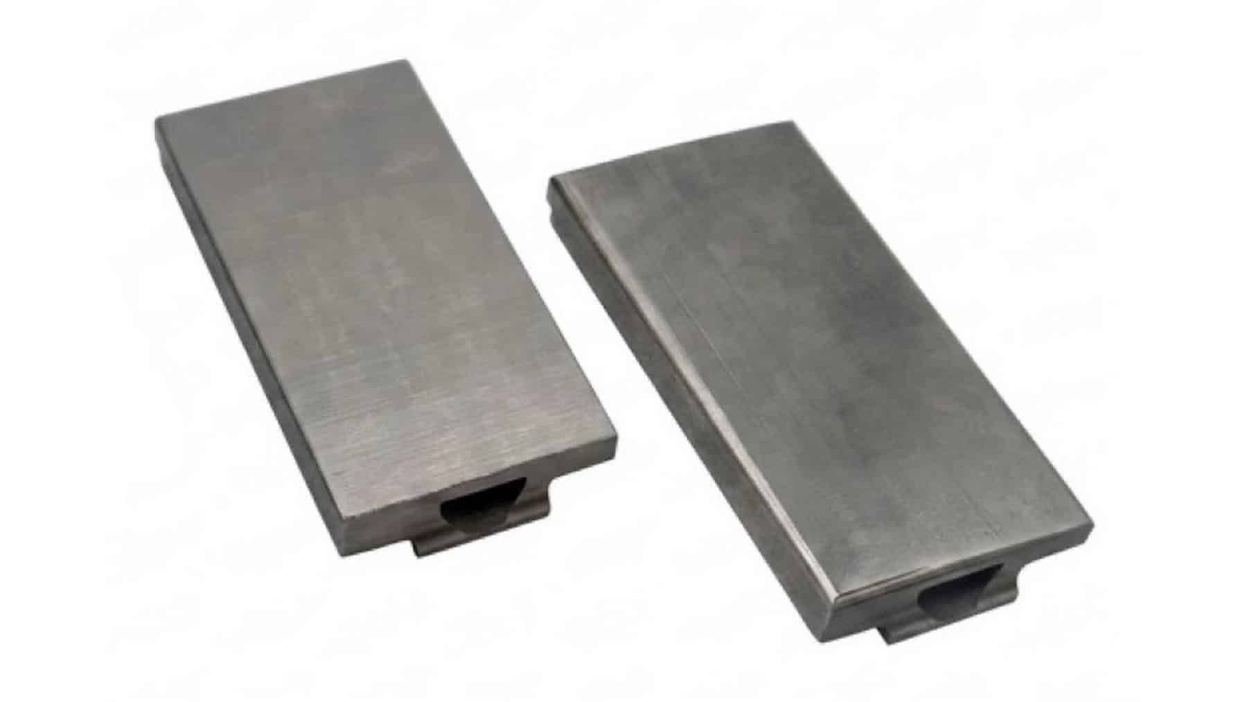
Now a team from North Carolina State University and Oak Ridge National Laboratory says it 3D-printed full-size tungsten tiles, bolted them into the bottom of a fusion machine in San Diego and reports that they survived 74 plasma shots intact. Japanese instrument maker JEOL printed the parts on its large electron-beam system. The partners announced the results on October 22, and the American Nuclear Society covered the campaign on November 5.
So why is tungsten so hard to work with?
Tungsten has a bit of a split personality. Above a certain temperature it behaves like a normal, somewhat bendy metal. Below it, it turns brittle, and for tungsten that switch happens somewhere between about 392°F and 1,112°F.
Which means at room temperature it acts more like a ceramic dinner plate than a metal. Hit it the wrong way and it can crack.
That makes tungsten tough to machine, tough to join and, as it turns out, tough to 3D print. Most metal printers use a laser to melt powder one thin layer at a time, and according to the researchers, most laser-printed tungsten has come out porous and full of cracks. Basically, each fresh layer cools off, drops into that brittle range and splits.
The NC State and Oak Ridge method swaps the laser for an electron beam. Electron-beam powder bed fusion still builds a part layer by layer from metal powder, but it does it inside a vacuum and uses a focused beam of electrons as the heat source. The beam keeps the surrounding material above 2,552°F the entire time, which is way above the point where tungsten turns brittle, which cuts the risk of the part cracking while it’s being made, though it doesn’t guarantee a crack-free build.
The two labs published the approach in the Journal of Nuclear Materials a few years ago, and Oak Ridge has kept developing it since. Other groups are attacking the same brittleness problem from a different direction, like the tungsten alloy out of the University of Birmingham that refines its own grains with heat alone.
These tiles are bigger than anything NC State had printed
Until this year, the printed tungsten was in sample form. Last year, NC State tested small tungsten “buttons” in the same San Diego machine using a sample holder called DiMES, and they came out with minimal surface damage. Those buttons saw heat loads of roughly 1.9 megawatts on every square foot, with brief spikes past 3.2 megawatts per square foot. Keep in mind those figures belong to the little buttons, not to the tiles in this story.
Then in December, Jonathan Coburn of Sandia National Laboratories, who led the novel-tile part of DIII-D’s tungsten tile testing campaign, invited the team to try a full-size tile. JEOL engineers Satoshi Ono and Akimine Hatsuda printed several flat and domed versions at the company’s Akishima, Japan, facility and adjusted the build after the first run.
The final pair measures about 5.35 by 5.63 inches and is roughly 0.79 inches thick, a hair over three-quarters of an inch. A standard DIII-D tile is about 5.5 by 5.1 inches, and the biggest tungsten part NC State had printed before this was about 2 inches across.
Nobody has published a weight for the tiles. If you run the numbers on a solid block the size of the pair, tungsten’s density puts it a little over 16 pounds, and the real parts weigh less because material was cut away for the mounts and the face was ground into a dome. Still, that’s a pretty hefty chunk of metal for something with roughly the footprint of a paperback book.
Printing only got the team part of the way there. Back at NC State, the researchers used wire EDM, which cuts metal with electrical sparks instead of a blade, to shape the mounting features and a gently domed face with a radius of about 3.3 feet. A spark doesn’t lean on a brittle part the way a cutting tool does, so it’s a sensible choice for tungsten. Then a multi-axis grinder, steered by a digital model of each tile, shaved roughly 0.01 inches off the side that faces the plasma and left it with a mirror-like finish.
According to the team, the whole thing took about eight months, from Coburn’s invitation to hardware sitting inside the machine. For a project spread across a university, two national labs and a company in Japan, that’s pretty quick.
So what’s a divertor?
DIII-D is a tokamak, a donut-shaped machine that uses powerful magnets to hold a plasma hotter than 180 million degrees Fahrenheit. General Atomics runs it for the Department of Energy. It doesn’t make electricity. It’s a research machine for working out how future power plants should be built, and it’s been busy lately, with Princeton researchers also running a machine-learning controller that reacts 50 times a second on it.
The divertor is basically the machine’s exhaust system. Heat and particles that escape the plasma get steered down onto the tiles that line the bottom of the vessel, and those tiles take a beating. According to the NC State team, ITER and the power plants that follow it will need that lining to handle a steady 1 to 2 megawatts on every square foot, with short bursts that go much higher.
In July, the two printed tiles went into DIII-D’s lower divertor, mounted on copper-alloy pedestals. NC State undergraduate Olivia Mehalick was in San Diego for the installation. Over three days, the tiles took direct plasma exposure through 74 shots in H-mode at medium to high power.
H-mode is short for high-confinement mode. It’s the setting where the plasma holds on to its heat much better, and it’s the way researchers expect future power plants to run, so you’d have to call it a fair test.
Added up, those 74 shots come to about four minutes of total plasma exposure. That works out to a little over three seconds per shot on average. Four minutes might sound a little underwhelming, and frankly, by power plant standards it is. But you’re looking at dozens of short, very hot hits rather than a few minutes of gentle warmth.
A neighboring tile melted, but don’t read too much into it
So how did the printed tiles do? They came out intact.
They also got an extra test nobody planned. One of the conventional tiles next to them was slightly misaligned, and its leading edge melted and spattered molten metal onto one of the printed tiles. A tile that isn’t sitting flush can catch heat on an edge its neighbors don’t, which is presumably what happened here. The printed pair came through that too, and marks from the melted tile are still visible around them.
It’s tempting to read that as printed tungsten beating the regular stuff. I’d be pretty careful with that. The conventional tile was out of position and the printed ones weren’t, so this was never a fair fight. Still, the printed material took a splash of molten metal and stayed in one piece, and the researchers describe the episode as an accidental bonus test.
Coburn, watching from DIII-D’s control room, told the team the printed tiles “performed really well,” at least as far as anyone could tell from there.
Detailed results haven’t come out yet
So what don’t we know? Quite a lot, honestly. The announcement doesn’t give a heat load for these full-size tiles, so I can’t tell you how hard they were hit compared with last year’s buttons. There’s also no measurement yet of how much tungsten wore away during the campaign. And the team hasn’t said how that conventional tile ended up out of position in the first place.
You won’t have to wait forever, though. The tiles are being pulled out, imaged and surface-scanned so the team can compare them with how they looked before going in, and JEOL’s own write-up of the project says the same. Until that comparison is done, “intact” is the main result, and it’s a visual one.
Oak Ridge’s Michael Kirka argues the tiles move 3D printing from a promising idea to a proven one for fusion parts. That’s arguably getting a little ahead of the data, given the analysis isn’t back. I get the enthusiasm, though. If printing holds up, labs could presumably make tungsten parts in shapes that’d be a real pain to carve out of a solid block.
The team presented the project at the AM2F conference in Cambridge, Massachusetts, on August 31, and JEOL put printed tiles on display at IMTS in Chicago in September. According to the October 22 announcement, the tiles go back to NC State for detailed analysis once DIII-D finishes a radiation survey on them.